

OTC: Jocienne Nelson: OC ’14, Director’s Postdoctoral Fellow at the National Renewable Energy Laboratory
Dr. Nelson’s research could increase efficiency in electronics.
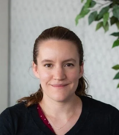
Dr. Jocienne Nelson, OC ’14, director’s postdoctoral fellow at the National Renewable Energy Laboratory, gave a talk on campus yesterday as part of the Physics and Astronomy Lecture Series. Nelson discussed atomic spray paint for renewable energy and energy efficiency.
This interview has been edited for length and clarity.
How did you get into this?
I did research here at Oberlin and that definitely got me interested. I worked with Professor of Physics Stephen FitzGerald in his lab, which got me interested in working. I’m a condensed matter physicist, which is a broad category of physics. I think doing research here and seeing research is kind of messy. It’s a lot harder and you don’t have straightforward answers, but that’s pretty fun. Beyond that, you can work on theoretical, very idealized systems, or you can be an experimentalist like me and work on real materials that are super messy. I think doing research here made me realize that I enjoyed that. Solid state systems are kind of messy. They have defects and disorders and nothing is perfect. It’s a complex system you have to solve, and that’s how I got into condensed matter physics.
I went to Cornell University for my PhD after Oberlin. I was initially interested in very basic research. A lot of the goals in my PhD were to understand materials that are adjacent to high-temperature superconductors; asking how we can understand the behavior of electrons and understanding how materials behave. With that, I worked with other groups at Cornell. I think one of the really fun things about being a scientist is that you can’t really do anything on your own, right? You have to collaborate with other people. I found it really exciting to help these groups work on things that could be part of fighting climate change, and that’s how I got interested in moving more toward applied research.
What is it that you’re researching?
I am researching new materials that could be used for things like energy-efficient electronics or renewable energy. Our group grows thin films. We grow these thin film materials on a substrate, and that’s a necessary step to make any sort of electronic device that goes into a chip in your computer. Physicists do material discoveries where they essentially make small rocks, and that’s great for finding new materials, but our step is to take those materials that have been discovered as tiny rocks and figure out how to make films out of them. Then we can do a lot of new and interesting physics with those films that couldn’t be done as small rocks.
Are there any limitations to this study?
The limitation is Moore’s Law. All of our current electronics are based on silicon, and silicon is probably the most well-studied material in human history. There’s been a ton of work, money, and effort put in over decades to make computer chips out of silicon, but we’re soon going to get to a point where devices are essentially becoming too thin. You get more efficiency the denser and smaller devices are, and that’s worked for a long time. You can have a computer in your phone, whereas it used to be a big room. However, because we’re getting to a point where everything is so thin, it’s starting to approach a few atomic layers. That’s kind of a fundamental limit for silicon. So, we need to move to and understand other materials.
What kind of elements or materials do you think will be the next big thing?
There are a lot of different candidate systems right now. It’s an exciting time to be in the field because there’s a ton of different things being studied. During my PhD, I studied transition metal oxides. Those are things like copper and oxygen, for example. Those systems are a push to create oxide electronics instead of silicon-based electronics. The systems are really cool because length skills are really short, so you can make ultra-thin devices out of them. Another aspect is that there are electrons in a chunk of copper, for example, and they don’t really ever talk to the other electrons, but in transition metal oxides, the electrons strongly interact with each other. That creates mini body physics, and it’s easy to understand the interaction of two particles, but three particles or more, it’s very difficult. It creates a lot of super interesting behavior that just comes as a result of collective behavior of electrons. Those are transition metal oxides.
What I’m studying now are topological materials. These materials are related to semiconductors, so we can grow them in the same chambers that we grow gallium arsenide, which is a very common semiconductor. They’re materials that like certain aspects of the electronic structure or the way the electronics interact, and they are very robust to defects and disorder. You can have a ton of disorder that is naturally occurring in any sort of fabrication process but still have really great metrics for material quality. Those are also pretty promising.
What are semiconductors?
I don’t specifically work on semiconductors, but you can think of semiconductors as the building blocks for electronic devices or the materials that we make to create devices like transistors. The physics description would be that you have an insulator, it has a large band gap, it doesn’t connect or conduct electrons very well. Or you have a metal where they conduct electrons very easily. A semiconductor is kind of in between and ends up being a useful building block for devices.
Do you think that these new types of materials can help improve climate change?
I definitely hope so. I don’t think I have great metrics for that, but everything we’re working on will have that goal. However, it’s a big field and there are a lot of different problems to work on. Right now, we’re exploring different spaces and different material systems, but I really hope it will have an impact.
What do you think the next couple years of research will bring?
We have basically figured out how to grow the material that I’m talking about today — a prototypical example of a topological semimetal. I’m hoping that we can start collaborating with a lot of different groups to make devices out of these materials. At the same time, we hope it further optimizes the growth and think about the other material systems we can work on. However, I think the really exciting thing is that we’ve grown it; what can we do with it and who can we send it to so they can do interesting science with these materials?
Another huge goal for us is to understand how defects and disorders caused by material growth impacts properties, because that has implications beyond this one material that we’re growing. We can apply it to a broad range of topological materials that could potentially be useful to a whole community of scientists who are trying to take these materials and apply them.


